Console and process jumps, why it matters and what it could bring to the PS5 Slim and PS5 Pro
August 16, 2023
0
Semiconductor manufacturing nodes or processes are a key part of the technology sector that generally affects all devices and products that are led by a chip. As is
Semiconductor manufacturing nodes or processes are a key part of the technology sector that generally affects all devices and products that are led by a chip. As is evident, consoles are no exception, and according to the latest information, everything points to the fact that the PS5 Slim and PS5 Pro they could make a jump in the production node compared to the PS5.
We have two theories, the first one says that he will use PS5 Slim and PS5 Pro TSMC’s 3nm node, and the second ensures that both will be based on TSMC’s 5nm node. The truth is that the second one is more realistic for two very simple reasons, the high cost of TSMC’s 3nm node wafer and the high demand for it.
If Sony decides to go for the 3nm node to produce the APUs of both consoles, it will have to assume high wafer costs, and thus an increase in chip cost that might not compensate you despite the more chips you could get per wafer, and at the same time you would have to assume that due to the high demand for said node, you could suffers from a certain lack of supply, something that would no doubt be very damaging to the Japanese company as it could hinder its sales.
5 nm node is characterized by a lower cost per wafer, it is more mature, which means it has a very good success rateand Sony also wouldn’t have to compete so hard with the other tech giants to get a good supply level, so in general this node would be the best choice to make the APUs that the PS5 Slim and PS5 Pro will mount.
Process jumps: what difference they would make on PS5 Slim and PS5 Pro
Process jumps or manufacturing nodes in semiconductors mean a reducing the size of transistorswhich normally allows increase their density per square millimeter. These leaps improve design efficiency and performance, and also reduce the space occupied by each chip on the wafer, so more chips can be achieved with a smaller node.
Improving the ratio of performance and consumption it depends on each nodeand it can also vary depending on the generation we’re comparing it to, as there are standard and enhanced versions in each node. For example, TSMC has both a standard 5nm node and an upgraded node that is labeled N4P and is mistaken for a 4nm node by some.
However, as I said before, a more advanced node has a higher economic cost, meaning wafers are more expensive, and while it allows you to get more chips per wafer, it also increases the risk of more broken chips. from reducing the size of transistors increases the probability of failure of logic gates.
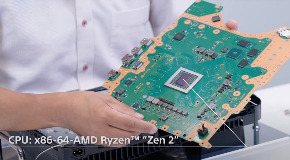
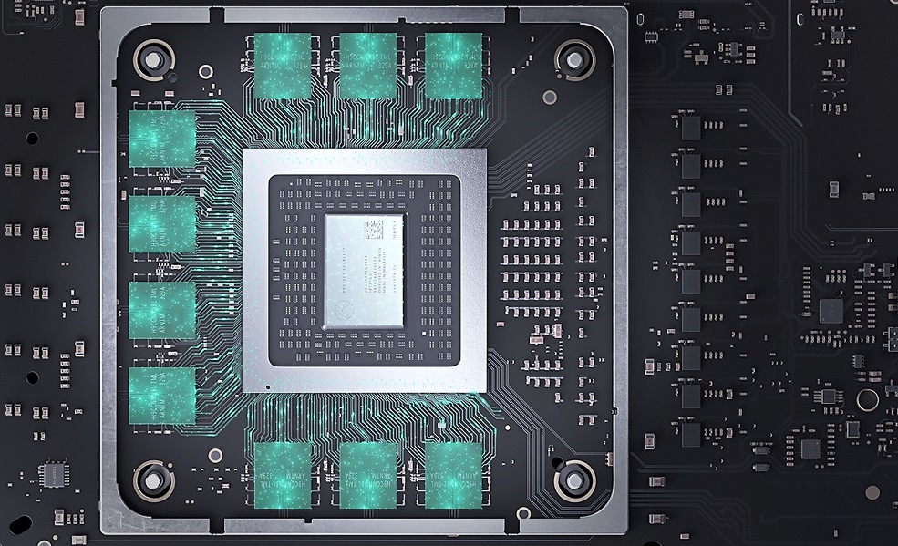
Therefore, go to a more advanced node It has its advantages, but also disadvantages.and for this reason, it is not always best to resort to the front node, but to the one that offers the best value in terms of performance, efficiency, success per wafer and cost. For this reason, Sony decided to use the 7nm node on the PS5 and later jumped to the 6nm node with the Oberon APU used in the last revision of the said console.
On the PS5 Slim and PS5 Pro, Sony will most likely opt for a 5nm node because eventually It is the one that offers the best relationship in all the keys we have givenand in general, it would be more than enough to achieve an optimal implementation of the new GPU that the PS5 Pro will bring, which will theoretically have 3,840 shaders. In comparison, the Xbox Series X GPU has 3,328 shaders and is manufactured on a 7nm node.
Thanks to the jump to the 5nm node of the PS5 Slim GPU it will consume less and burn less, but maintain the same level of performance than the one using the PS5 and should have a lower average production cost. In the case of the PS5 Pro, its GPU manufactured in 5 nm will allow to integrate a greater number of shaders without taking up space at the silicon level, maintaining a good relationship between performance, consumption and generated heat. I don’t think the TDP will exceed 200 watts.
So when will we see the jump to the 3nm node on consoles?
Most likely, both Sony and Microsoft will reserve such a node for the next generation of consoles. Both the PS4 and Xbox One used APUs based on the 28nm nodeand the PS4 Pro and Xbox One X made the jump 16nm node. It was an important and quite significant leap, allowing to mount a much more powerful GPU while maintaining a manageable TDP and a balanced cost.
The PS5 and Xbox Series X use a 7nm node, so the jump to a 3nm node in their next generation makes sense because we’re talking about more than 50% reduction and an important development compared to the current generation.
I know that if we get carried away by the numbers, this development may seem less striking, but we have to consider that with the 3 nm node, we are very close to the theoretical limits of silicon, making it increasingly difficult to continually reduce the size of transistors. Simply put, going from 28nm to 16nm was much easier than going from 7nm to 3nm, and going further down will be very difficult.
Donald Salinas is an experienced automobile journalist and writer for Div Bracket. He brings his readers the latest news and developments from the world of automobiles, offering a unique and knowledgeable perspective on the latest trends and innovations in the automotive industry.


![[adv] MSI Back 2 School: All about these powerful business laptops](https://itdaily.be/wp-content/uploads/2023/08/MSI_Modern_15_Classic_Black_5.jpg "[adv] MSI Back 2 School: All about these powerful business laptops")


