Scientists announce discovery of two-dimensional waveguides
February 23, 2024
0
The US Naval Research Laboratory (NRL), working with Kansas State University, announced the discovery of plate waveguides made of two-dimensional hexagonal boron nitride material. This milestone was documented
The US Naval Research Laboratory (NRL), working with Kansas State University, announced the discovery of plate waveguides made of two-dimensional hexagonal boron nitride material. This milestone was documented in a magazine Advanced Materials.
Two-dimensional (2D) materials are a class of materials that can be reduced to a single layer boundary by mechanical exfoliation of the layers. Weak interlayer attraction, or van der Waals attraction, allows layers to be separated using the so-called “secretary tape” method. Graphene, the best-known two-dimensional material, is a semi-metallic material consisting of a single layer of carbon atoms. Recently, other 2D materials have also attracted attention, including semiconductor transition metal dichalcogenides (TMDs) and insulating hexagonal boron nitride (hBN). When reduced near the monolayer boundary, 2D materials have unique nanoscale properties that are attractive for creating atomically thin electronic and optical devices.
Unexpected optical properties
from the Department of New Materials and Applications. “While we knew that using hexagonal boron nitride would lead to extraordinary optical properties in our samples, none of us expected that it would also act as a waveguide,” said Samuel Lagasse. “Since HBN is so widely used in 2D material-based devices, this new use as an optical waveguide has potentially broad implications.”
Graphene and TMD monolayers are extremely sensitive to the environment. Therefore, researchers tried to protect these materials by encapsulating them with a passivating layer. This is where hBN comes to the rescue: hBN layers can “shield” impurities near graphene or TMD layers, offering fantastic properties. In a recent study conducted by NRL, the hBN thickness surrounding the light-emitting layer of the TMD was carefully tuned to support optical waveguide modes.
Advances in waveguide technology
Researchers at NRL carefully assembled two-dimensional packages of materials known as “van der Waals heterostructures”. These heterostructures may have special properties due to layering. hBN sheets were placed around individual layers of TMDs such as molybdenum diselenide or tungsten diselenide, which emit light in the visible and near-infrared ranges. The thickness of the hBN sheets was carefully adjusted so that the emitted light was trapped inside the hBN and guided by the waveguide. When the waveguides shine light on the edge of the hBN, it scatters and can be detected by microscopy.
The work was motivated by problems in optical measurements of 2D TMD. When laser light is focused on a TMD, particles known as excitons are produced. Most excitons emit light from the TMD plane, but in some TMDs there is an elusive type of exciton known as a “dark” exciton that emits in the TMD plane. NRL layered waveguides capture light from dark excitons, providing a way to study them optically.
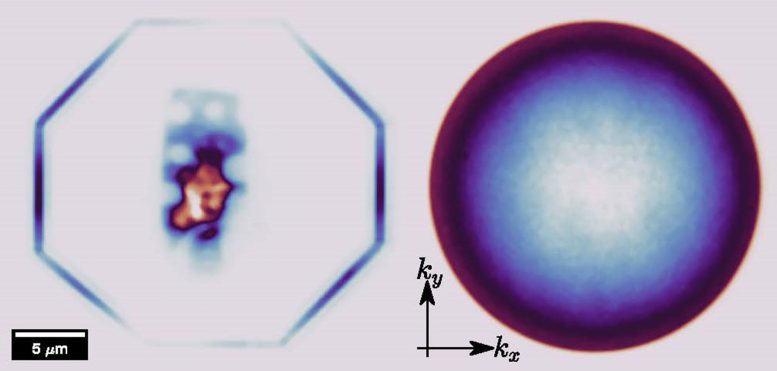
Photoluminescence image of hexagonal boron nitride waveguide in real space (left) and Fourier space (right). The real space image shows where the photoluminescence is emitted in the sample, while the Fourier space image shows the angle of the emitted light.
“2D materials have exotic optoelectronic properties that will be useful to the Navy,” Lagasse said. “The biggest challenge is to combine these materials with existing platforms without damaging them; these boron nitride waveguides are a step towards this realization.”
NRL researchers used two special types of optical microscopes to characterize hBN waveguides. One setup allows researchers to spectroscopically distinguish photoluminescence emitted from different points in the waveguide. Another setup allows you to observe the angular distribution of the emitted light.
NRL researchers also developed three-dimensional electromagnetic models of the waveguides. The simulation results provide a set of tools for designing future 2D devices using plate waveguides.
As an experienced journalist and author, Mary has been reporting on the latest news and trends for over 5 years. With a passion for uncovering the stories behind the headlines, Mary has earned a reputation as a trusted voice in the world of journalism. Her writing style is insightful, engaging and thought-provoking, as she takes a deep dive into the most pressing issues of our time.