2D “antenna” increases light emission from carbon nanotubes
- March 24, 2024
- 0
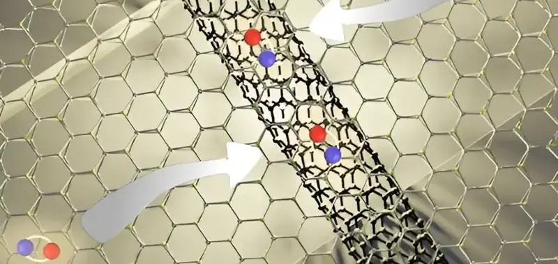
The flat sheet of atoms can act as a kind of antenna, absorbing light and directing its energy into the carbon nanotubes, making them shine brightly. This advance
The flat sheet of atoms can act as a kind of antenna, absorbing light and directing its energy into the carbon nanotubes, making them shine brightly. This advance

The flat sheet of atoms can act as a kind of antenna, absorbing light and directing its energy into the carbon nanotubes, making them shine brightly. This advance could help develop small light-emitting devices that can exploit quantum effects.
Carbon nanotubes resemble very thin hollow wires that are only about one nanometer in diameter. They can produce light in different ways. For example, a laser pulse can excite negatively charged electrons within a material, leaving positively charged “holes”. These opposing charges can combine to form an energetic state known as an exciton, which can travel relatively far along the nanotube before releasing its energy as light. In principle, this phenomenon can be used to create highly efficient nanosized light-emitting devices.
Unfortunately, there are three obstacles to using lasers to create excitons in carbon nanotubes. First, the laser beam is typically 1000 times wider than the nanotube, so the material actually absorbs very little of its energy. Second, the light waves must be perfectly aligned with the nanotube in order to transfer their energy efficiently. Finally, electrons in a carbon nanotube can only absorb light of a very specific wavelength.
To overcome these limitations, a team led by Yuichiro Kato of RIKEN’s Nanoscale Quantum Photonics Laboratory turned to another class of nanomaterials, known as 2D materials. These flat sheets are only a few atoms thick, but they can be much wider than a laser beam and are much better at converting laser pulses into excitons.
The researchers grew carbon nanotubes on a trench cut from insulating material. They then placed an atomically thin sheet of tungsten diselenide on top of the nanotubes. When laser pulses hit this wafer, they produce excitons that travel within and along the length of the nanotube before emitting light with a longer wavelength than the laser. It took only about a trillionth of a second for each exciton to pass through the two-dimensional material into the nanotube. The article was published in the magazine Nature Communication.
By testing nanotubes with different structures that affect important energy levels in the material, the researchers identified ideal nanotube shapes that facilitate the transfer of excitons through the 2D material.
Based on this result, they plan to use bandgap engineering, a useful concept in semiconductor engineering, to create devices with remarkable properties at an atomically thin scale. “When bandgap engineering is applied to low-dimensional semiconductors, new physical properties and innovative functions are expected,” says Kato.
“We hope to use this concept to develop photonic and optoelectronic devices as thin as a few atomic layers,” adds Kato. “If we can reduce these to the atomically thin limit, we expect to see new quantum effects that could be useful for future quantum technologies.”
Source: Port Altele
As an experienced journalist and author, Mary has been reporting on the latest news and trends for over 5 years. With a passion for uncovering the stories behind the headlines, Mary has earned a reputation as a trusted voice in the world of journalism. Her writing style is insightful, engaging and thought-provoking, as she takes a deep dive into the most pressing issues of our time.