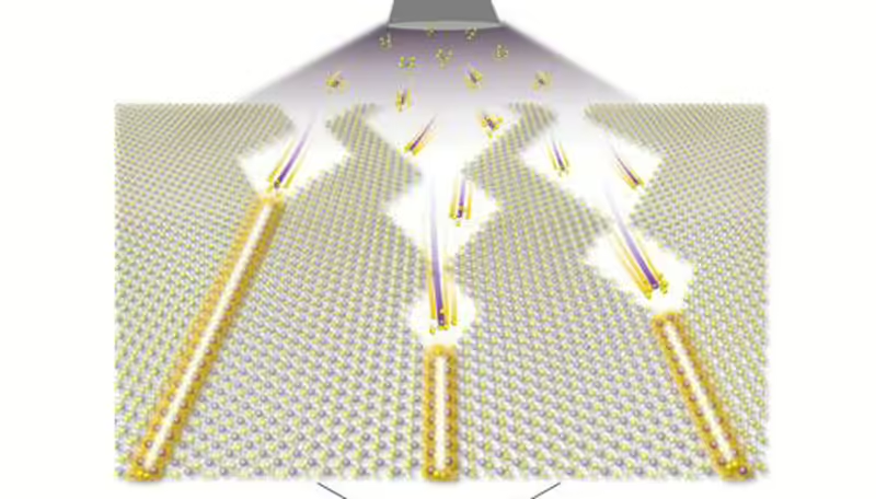
According to IEEE’s long-term plans, the semiconductor industry will master lithography with a 0.5nm pitch (node) with a gate transistor width of 12nm by 2027. South Korean scientists today have the opportunity to produce smaller transistors without waiting for the development of lithographic scanners. Using the new development, they learned to create a 0.4nm wide gate electrode without scanners to work with a 3.9nm wide transistor channel.
The detection of defects in the crystal structure of molybdenum disulfide (MoS₂) aided this discovery. ) . Under certain conditions, defects can be transferred to the metal phase in a controlled manner. This resulted in a 0.4 nm wide metal electrode on the wafer that no scanner can reproduce today or 15 years from now. The defect appears at the edge of the mirror separation between regions of the growing MoS2 crystal substrate ₂ By controlling the epitaxial growth of the substrate, it is possible to transform the interface into a one-dimensional thin metal electrode.
Scientists from the van der Waals Center for Quantum Solids at the Institute of Fundamental Sciences (IBS) in Daejeon have not only demonstrated the possibility of growing one-dimensional metals, but have also created two-dimensional field-effect transistors and even experimental chips with them. It turned out that a gate electrode with a width of 0.4 nm can create a 3.9 nm wide field (which controls the conductivity of the gate). Moreover, despite the atomic width of the channel, such a transistor showed excellent electronic conductivity and would therefore be effective for use in microcircuits.
Since the proposed transistors are incredibly simple in structure, they will not have parasitic capacitances that suffer from new-fashioned transistors, especially those with circular gates, and older FinFETs. This will provide additional gains in switching speed and energy efficiency.
Project manager Jo Moon-Ho said: “The one-dimensional metal phase obtained by epitaxial growth is a new material fabrication process that can be applied to ultra-miniaturized semiconductor processes. It is expected to be an important technology in the development of various low-power and high-performance electronic devices in the future.”


