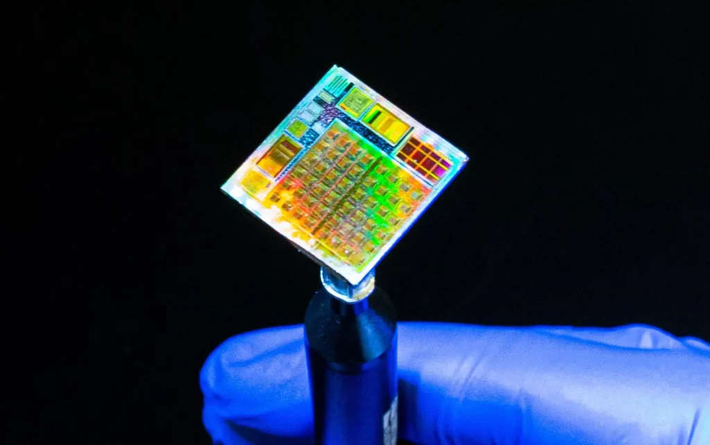
Semiconductors are small microcircuits used in almost all electronic devices. They are indispensable to our modern technology and are used in everything from smartphones to TV remote controls. During the pandemic, there was a global shortage of semiconductors. This has caused production difficulties for many industries and has led to higher prices for electronic devices. Fortunately, the chip shortage is long gone. And researchers are already working on new ways to improve this technology. Recently, researchers at King Abdullah University’s Department of Science and Technology developed a new microchip that uses two-dimensional (2D) materials to improve performance. Details are here…
Two-dimensional microcircuits based on materials could revolutionize electronics
Researchers at the King Abdullah University of Science and Technology (KAUST) have developed a new type of microchip that uses two-dimensional materials. 2D materials are incredibly thin, and some are only an atom thick. This makes them very strong and light, and they also have unique electrical and optical properties.
However, the integration of 2D materials into electronic devices has been challenging due to their fragility and difficulty to manufacture on a large scale. The KAUST team overcame these challenges by developing a new method for transferring 2D materials to microchips. Researchers who made a statement on this subject describe their work as follows:
“Our motivation was primarily to improve the technology readiness of 2D electronic devices and material-based circuits using traditional silicon-based CMOS chips and standard semiconductor fabrication methods. The problem, however, is that synthetic 2D materials are localized such as atomic impurities that can cause small devices to fail. “It can contain imperfections. It’s also very difficult to integrate a 2D material without damaging the microchip.”
“We fabricated a 2D material (hexagonal boron nitride or h-BN) on copper foil and transferred it to the microchip using a low-temperature wet process, and then built the electrodes on top using conventional vacuum evaporation and photolithography processes that we have in-house. In this way, a transverse “We created a 5×5 cell array with a matrix-connected transistor/a memristor.”
The team is currently working to improve the performance and scalability of the microchips. They are also exploring new application areas of this technology. The team believes the microchips could be used in a variety of applications, including; Wearable devices, flexible displays, artificial intelligence chips, medical devices, energy harvesting sensors and security systems. However, we emphasize that we still have more time for these activities.


