As I have told you on previous occasions, we are getting close theoretical limit of silicon. This means that every reduction in the production process becomes more and more challenging, and problems arise that can only be solved by major innovations, a reality that the chip giant has been able to respond to. Intel Power Via.
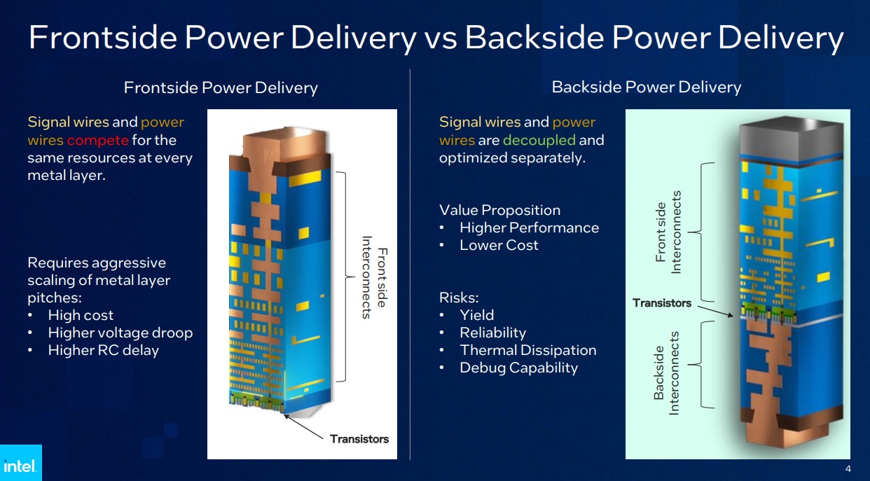
Let’s start from the beginning, what is Intel PowerVia? This is a technology that was started to be applied by the Santa Clara company implement a silicon-level power system at the back of the chip. This presents important differences compared to the classic front feed system because:
- Improves performance by up to 6% in the first tests Intel conducted with the Blue Sky Creek chip, based on the Crestmont architecture (the same as the high-performance Meteor Lake processor cores will use).
- Reduces voltage fluctuations by 30%minimizing peak peaks and thus achieving much more efficient operation.
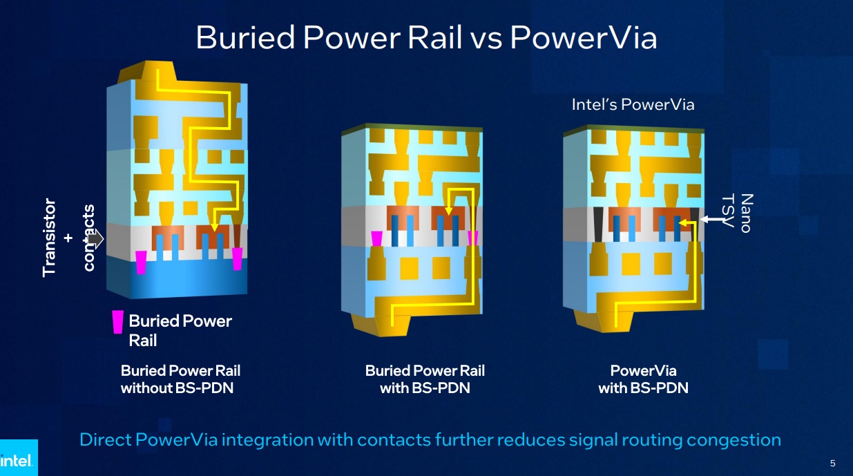
- Addresses bottlenecks that occur at the interconnect level, and which are primarily motivated by the integration of smaller, denser and more powerful transistors. Until now, the power and signal lines present in the transistor have to “fight” for the same resources. By separating them, we were able to increase performance and power efficiency, which is why this move from the power delivery system to the back of the chip is so important.
- It allows you to increase the density of transistors without having to sacrificeand maximize the performance and performance that a particular architecture could offer under a next-generation node.
Intel PowerVia is not a good idea on paper, It’s something that has already been carried over into the real worldand the first tests carried out by the chip giant with this Blue Sky Creek processor were satisfactory as they found no problem and verified that the temperature readings were completely optimal.
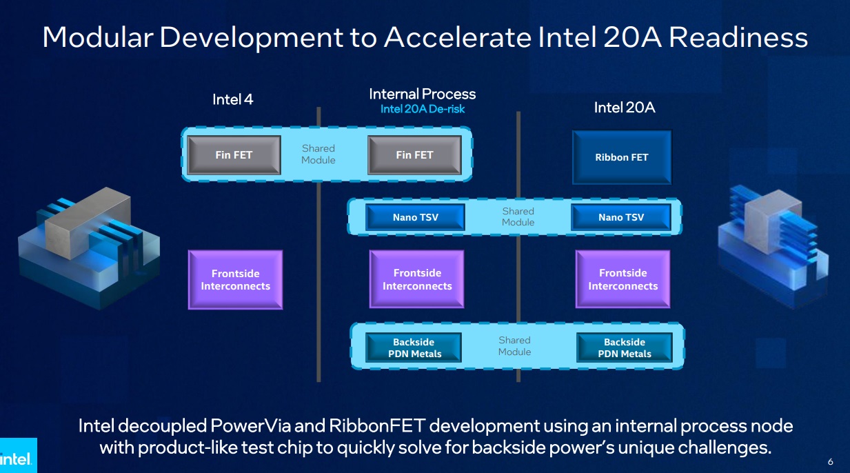
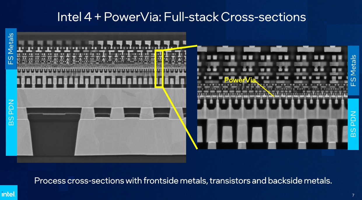
According to Intel, the development of PowerVia was separated from the development of transistors to guarantee its preparation for the implementation of its most advanced nodes, specifically in Intel 20A and Intel 18A (2 nm and 1.8 nm, respectively). The first test of PowerVia technology was carried out on the Blue Sky Creek chip RibbonFET made on an intel 20A node.
We’ve already seen some of the results Intel got, a 6% performance improvement and 30% lower voltage fluctuations, but that’s not all, the chip giant also said that cell utilization was over 90% and what he achieved significant reduction of transistors.
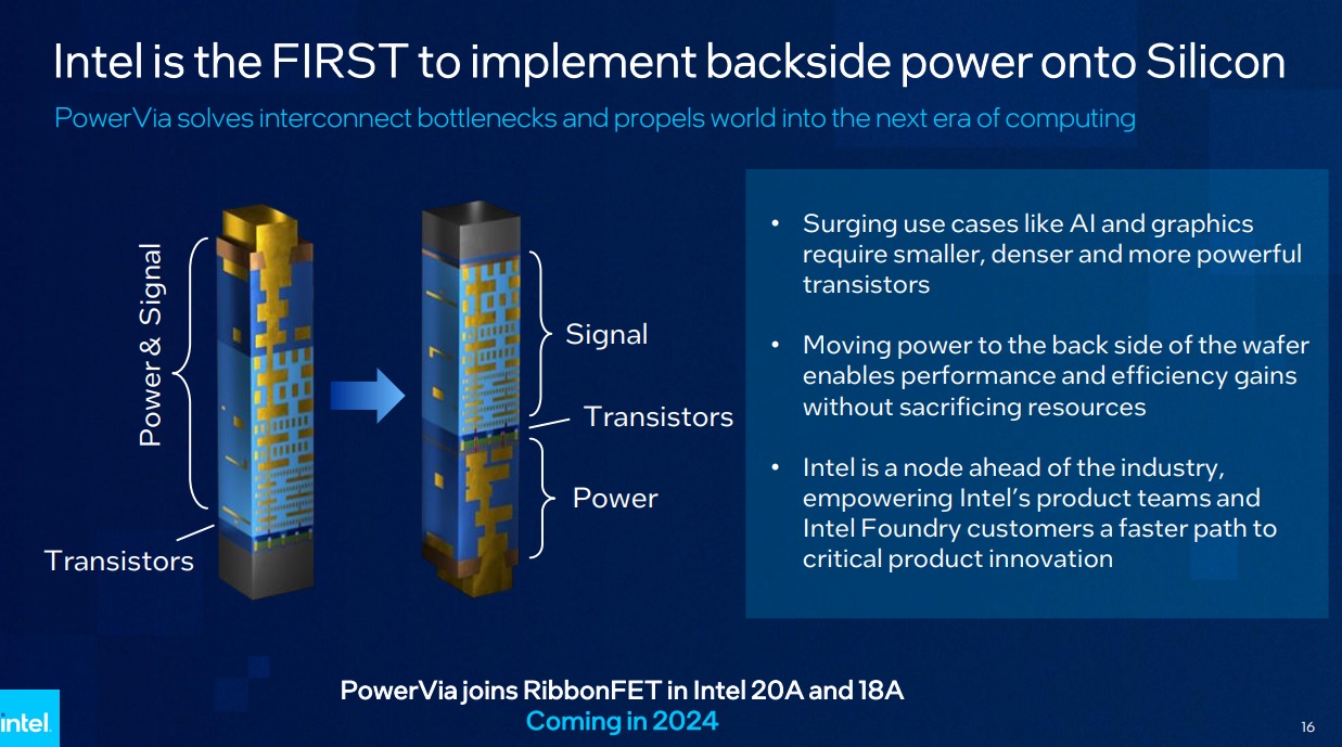
Intel PowerVia technology it will be introduced with Intel 20A and Intel 18A nodes, and these will also come with RibbonFET gate-all-around technology. The chip giant has already had all the problems this plan is planning on a thermal and debug level, and obtained very valuable data from this first test, which allowed it to confirm that this is a perfectly viable evolution, both for transistor scaling and for the rest. values.